Economic effects of sports events
In recent years, Chinese brand products have frequently appeared in top international competitions, with increasingly diverse and in-depth methods. The upcoming Paris Olympics will feature a large number of Chinese products, from sports equipment to Olympic licensed merchandise. Improvement of product quality and performance system. International top-level events are not only arenas for athletes from various countries, but also arenas for the quality and performance of products from different countries. China is deeply implementing the innovation driven development strategy, and the manufacturing industry has achieved significant results in new technologies, new materials, new processes, high-end equipment, etc., which has continuously improved the quality and performance of Chinese manufacturing products. The characteristics of high-end, intelligent, and green are more prominent, further enhancing its competitiveness in the global market, including international sports events. Made in China is renowned for its efficient manufacturing, complete supply chain system, and high-level infrastructure support, which is in line with the diversity, safety, timeliness, and economic requirements of international events for material supply. The complete industrial system ensures that "Made in China" can cover various products required for international events, from keychain souvenirs and table tennis to sports tables and tracks, from cultural and sports equipment, sports equipment to sports shoes and clothing. The presence of "Made in China" can be seen everywhere. The 2024 Paris Olympics in France is approaching; The 2024 FIVB Beach Volleyball U19 World Championship will also be held from August 27th to September 1st at the West Square of Qinling Museum; The 2024-2025 International Ski Federation snowboarding and freestyle skiing Grand Ski Jumping World Cup will be held from November 29 to December 1 this year at the Shougang Ski Jumping in Beijing. The sports economy and related sport products brought about by this series of events have continued to heat up.
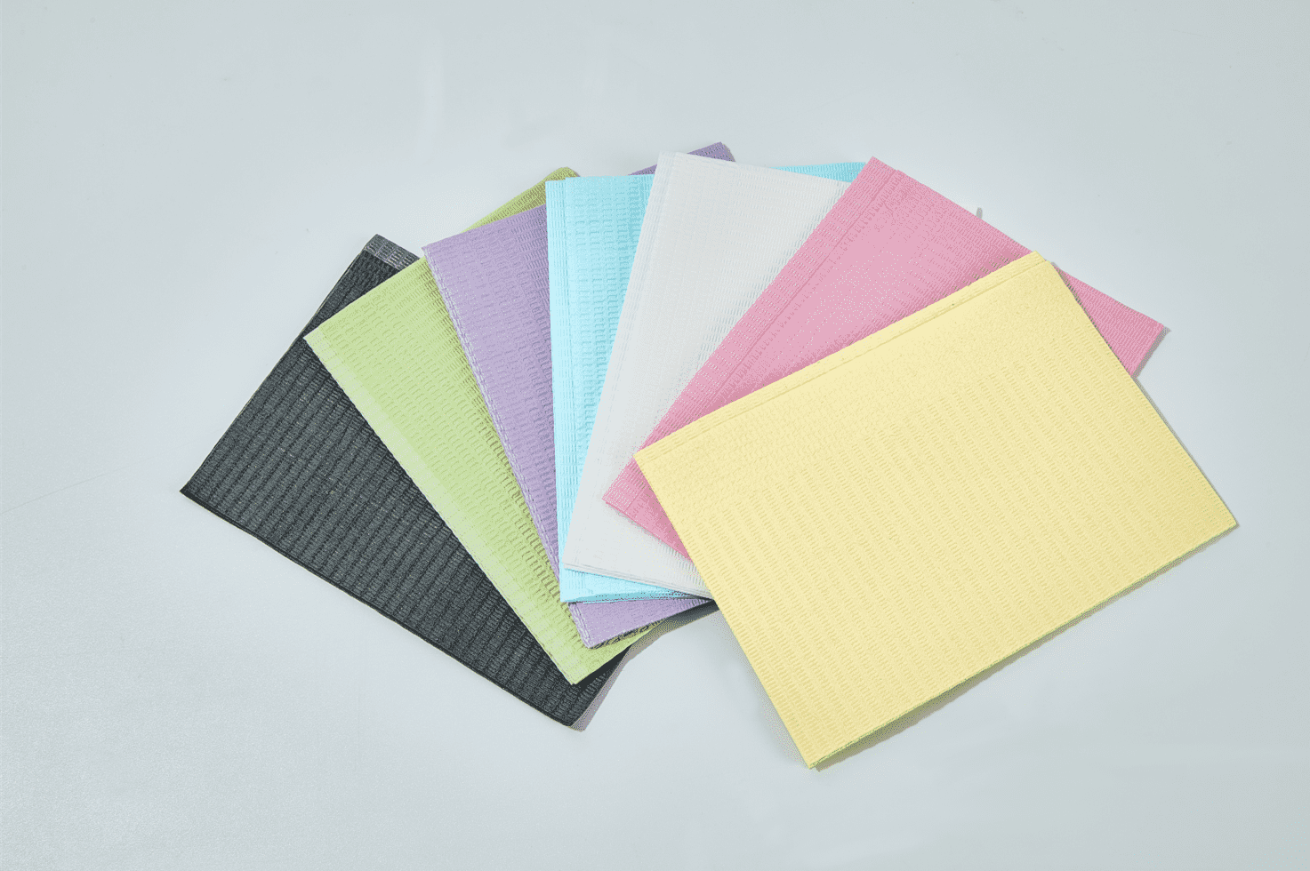
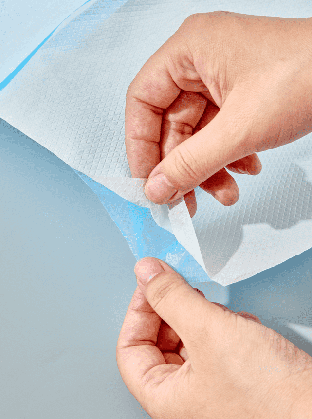
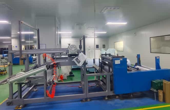
Xiamen Huakang Orthopedic CO LTD is a professional manufacturer of orthopedic braces and supports in China. These large-scale sports events have also brought business opportunities to these factories, which are busy producing various sports protective equipment and rehabilitation orthopedic equipment.Its products have all kind of adult orthotic braces with FDA and CE-MDR certification , including toe straps, figure 8 brace ankle support, ankle walking boot , dorsal night splint, plantar fasciitis foot braces, knee brace, sarmiento brace,hip abduction, lower back brace spinal support, clavicle brace and posture support, neck cervical collar, shoulder brace arm sling, humeral brace, wrist splint thumb spica, elbow splint , finger brace etc. Also we produce Children knee brace, kids arm sling, kids walker brace, kids sprained wrist brace ,children cervical collar etc.It still supply disposable medical face mask,kn95 face mask, medical face shield, medical protective isolation gown, medical safety goggles etc. If you want more information,please enter www.huakangortho.com.