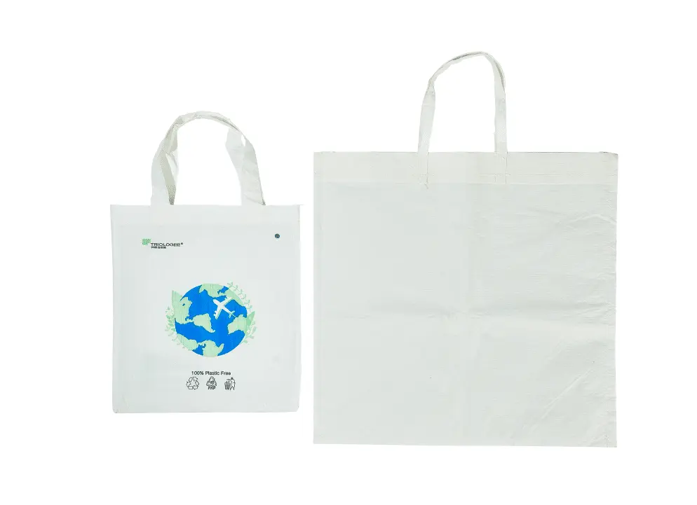
Sustainable Shopping The Benefits of Environmental Protection Shopping Bags
As the global push for eco-friendly solutions intensifies, businesses are increasingly turning to Environmental Protection Shopping Bags as a sustainable alternative to plastic bags. These bags not only reduce environmental impact but also offer exceptional durability, water resistance, and customization options, making them an ideal choice for brands that prioritize both functionality and sustainability.
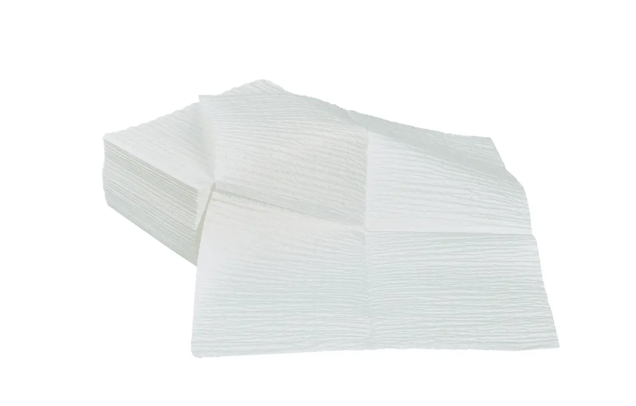
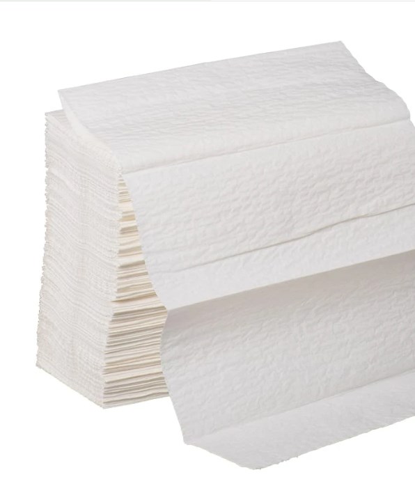
The Strength and Durability of Scrim Reinforced Hand Paper
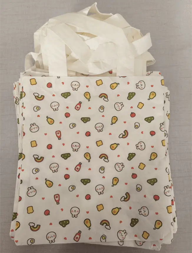
A key feature that sets these eco-friendly bags apart is their scrim reinforced hand paper construction. Made from pure wood pulp paper reinforced with a scrim mesh layer, this material provides superior tear resistance, enhanced flexibility, and remarkable durability. Unlike standard paper bags, those made with scrim reinforced hand paper are designed to withstand heavy loads without tearing, making them a reliable option for various industries.
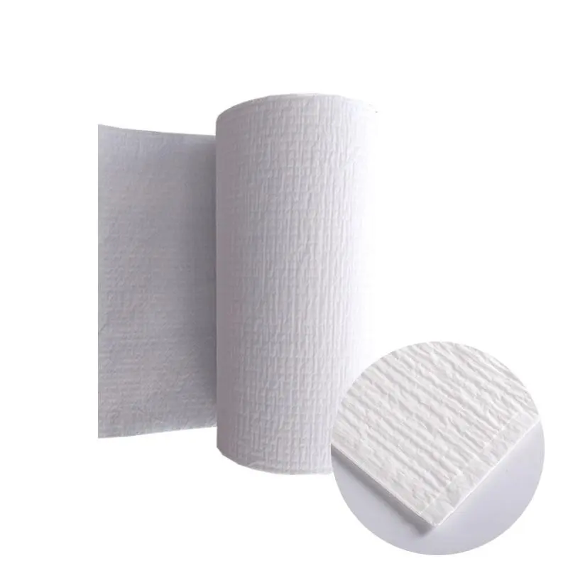
Scrim Paper: Waterproof and Eco-Friendly Innovation
One of the biggest concerns with paper bags is their vulnerability to moisture, but scrim paper solves this issue effectively. The unique composition of pure wood pulp paper with scrim mesh reinforcement creates a naturally water-resistant barrier, preventing the bag from weakening or disintegrating when exposed to liquids. This added water resistance ensures that the bag maintains its structure even in humid or wet conditions, making it a practical and sustainable alternative to plastic bags. Additionally, scrim paper is 100% biodegradable, providing an eco-conscious packaging solution without compromising on performance.
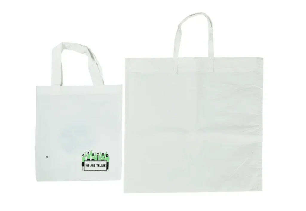
Why Choose Telijie Environmental Protection Shopping Bags?
For businesses looking for a high-quality, eco-friendly shopping bag solution, Telijie offers unmatched advantages. Our Environmental Protection Shopping Bags are crafted with pure wood pulp paper and scrim mesh reinforcement, ensuring superior strength, tear resistance, and water resistance. Additionally, Telijie provides customizable branding options, efficient order processing, and excellent customer service, making us a trusted partner in sustainable packaging.
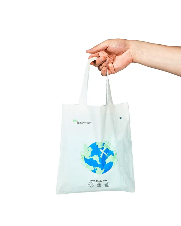
By choosing Telijie Environmental Protection Shopping Bags, you’re investing in a durable, waterproof, and eco-friendly solution that aligns with today’s sustainability goals. Make the switch today and elevate your brand’s commitment to a greener future!


")